Atomically Thin Circuits on Silicon
Overview
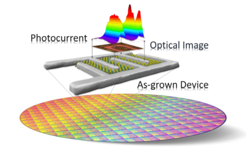
As Moore’s Law predicted, impending limitations in traditional CMOS technology led to a need for new innovation. The potential of two-dimensional (2D) materials, such as graphene, to both enhance existing technologies as well as provide new functionalities stimulated an explosion of research into these materials. In addition to characteristics such as extraordinarily high mobilities, semiconducting and superconducting behavior, ferromagnetism, and excellent thermal properties, many of these materials exhibit optical control of spin and valley degrees of freedom which may provide novel material-enabled functions in emerging areas such as spintronics or valleytronics. Despite this enormous potential, the inability to process material into working devices with any scalability is the largest impediment to capitalizing on the industrial promise of 2D materials. This technology has the potential to provide a scalable, front-end compatible, chemical vapor deposition (CVD) process to produce complex, conformal, as-grown, self-contacted 2D materials-based devices.
Published Patent application: US 2019/0131129 A1
OU Ref: 16025 View PDF
Inventor
Eric Stinaff, Ph.D. Associate Professor of Physics and Astronomy